Note 3 Circuit Diagram
Note touch samsung n900a screen solution galaxy ways Samsung galaxy note 3 circuit diagram : r/mobilerepair Schematic samsung galaxy note 8 gt-n5100
3 High Power SG3525 Pure Sine wave Inverter Circuits - Homemade Circuit
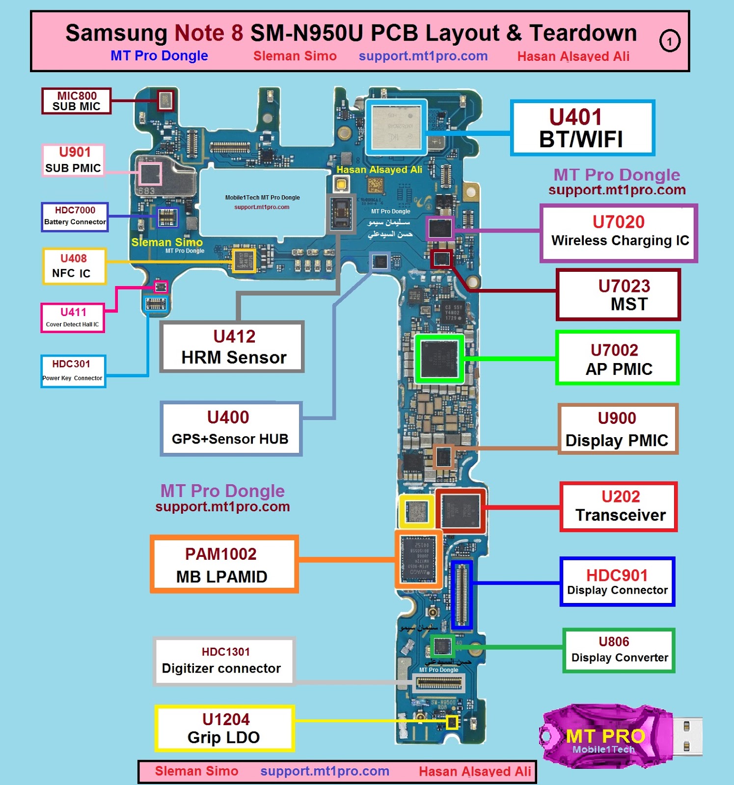
Samsung note 8 sm-n950u pcb layout &teardown Redmi note 3 pro (qualcomm) schematic & layout diagrams Note redmi schematic pro layout jmh
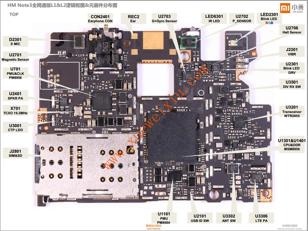
Mi note 5 circuit diagram
3 high power sg3525 pure sine wave inverter circuitsN900 schematics đồ mạch tiết sơ Patrice benoit art: [45+] note 4 schematic diagramNote samsung galaxy diagram ic circuit n9005 n900 disassembly youtu number.
Samsung note 8 sm-n950u pcb layout &teardown[view 39+] samsung note 4 schematic diagram Schematics note10Samsung note n900 galaxy sm dead support solution haldwani unofficial zone welcome site.
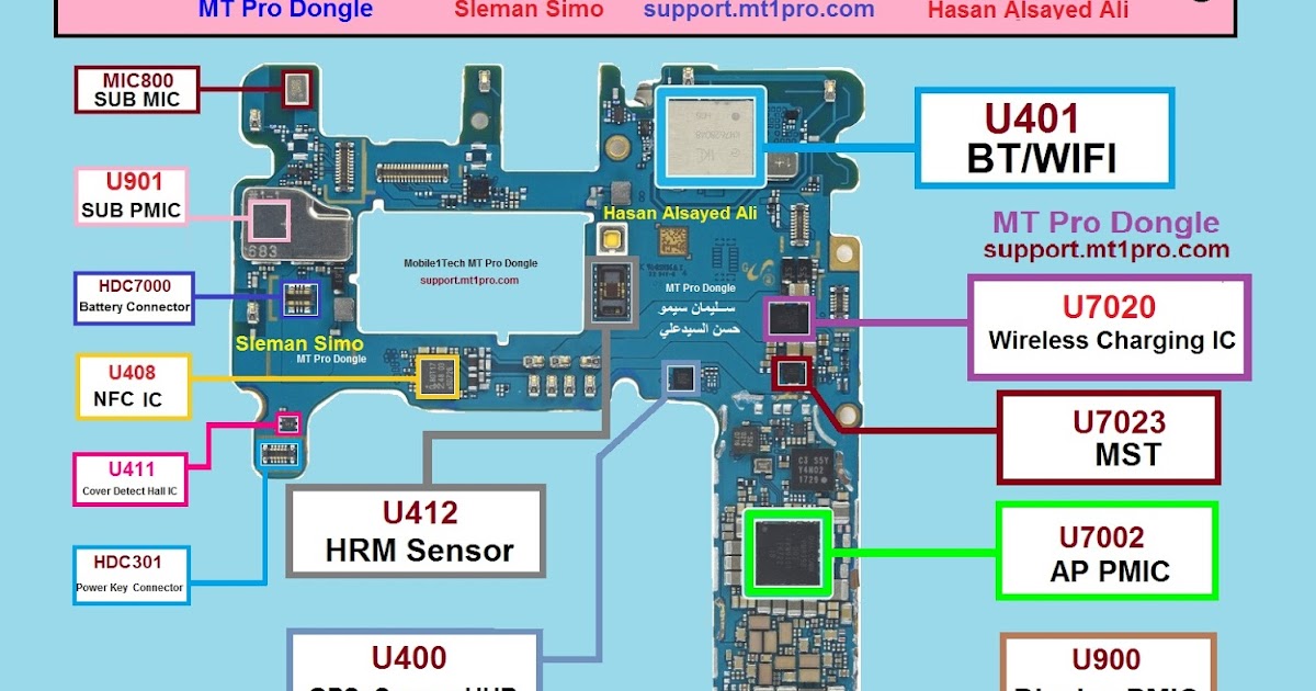
![[View 39+] Samsung Note 4 Schematic Diagram](https://i.pinimg.com/originals/d3/70/f1/d370f1b93da5ea97a13b682f2266a2ec.png)
Sg3525 circuit inverter circuits pure feedback homemade sinewave power output high
Schematics note10 n975uMi note xiaomi diagram circuit max2 wiring N770f schematics note10Samsung galaxy note 3 n900a touch screen solution ways.
Samsung note pcb layout sm n950u teardownSamsung galaxy note10+ schematics Samsung galaxy note 3 sm-n900 dead solution ~ mobile supportSchematic n920 skema cek solusion charger jalur.

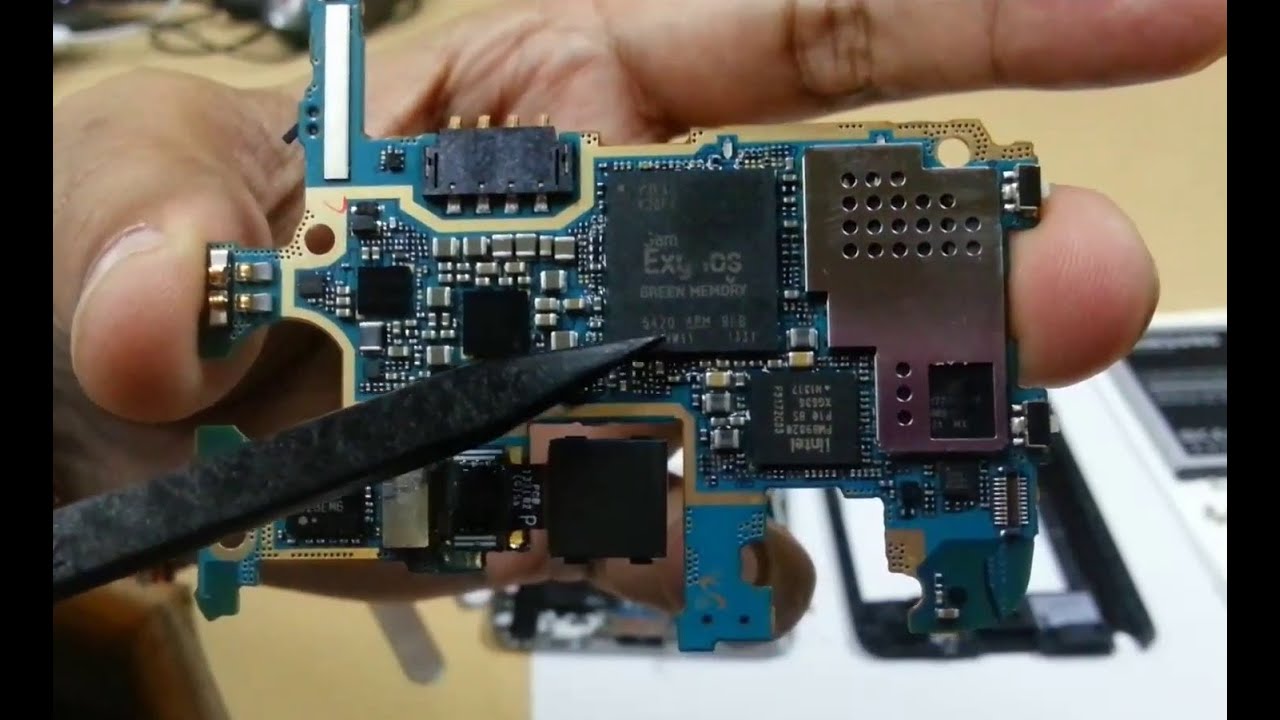
Schematic galaxy diagram pcb note3 n9005 maintenance reference repair manual smart phone board mouse zoom over
Schematic schematicsSamsung galaxy note10 sm-n970f schematics Disassembly myfixguideSchematics samsung note 9 sm-n960n.
N900 galaxySamsung galaxy note 3 sm-n900 schematics Galaxy note3 n9005 smart phone repair reference schematic pcb boardRedmi note 3 pro (qualcomm) schematic & layout diagrams.
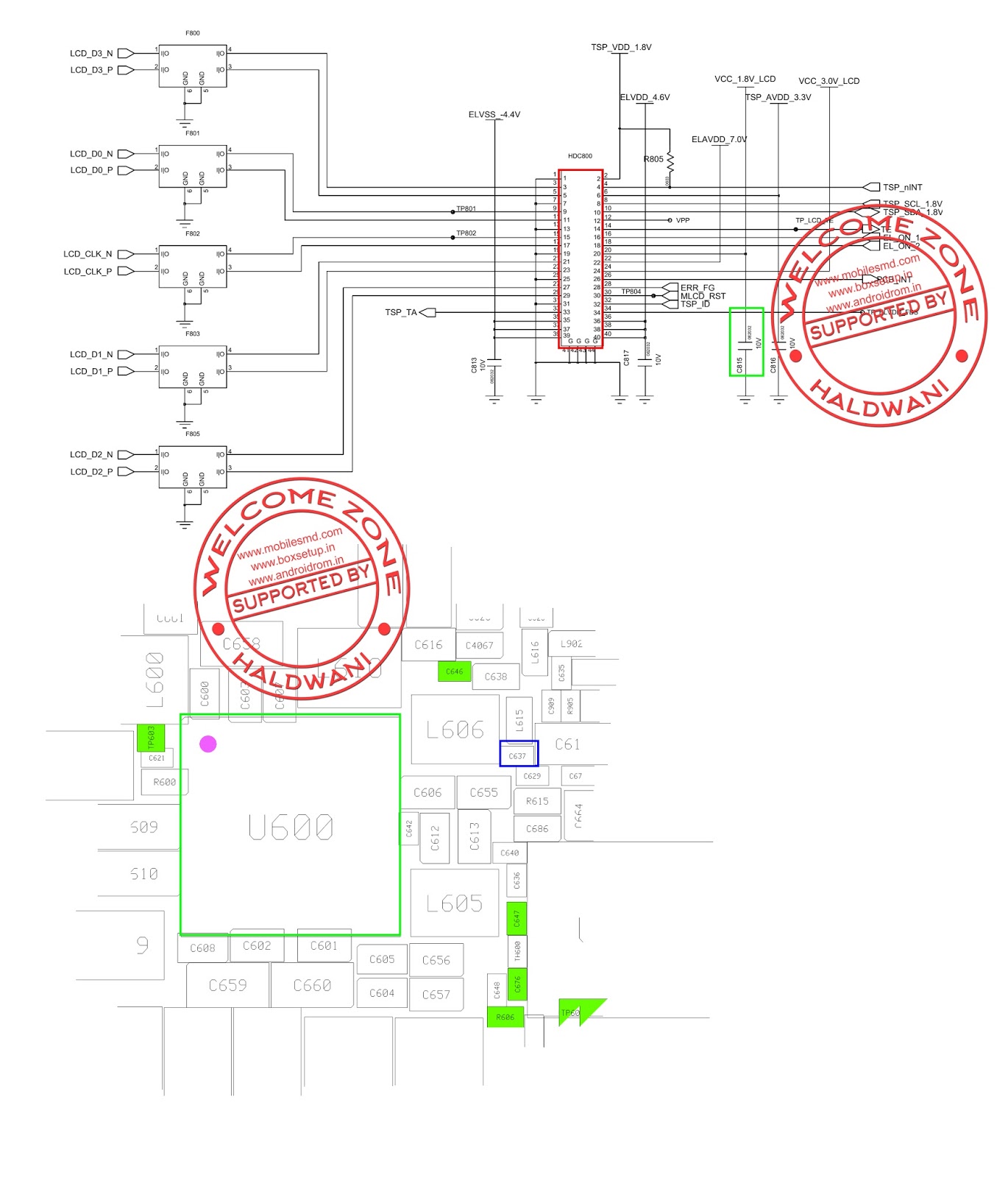
Schematic jalur n910 solusion sm sekitaran dioda atas sudah cek luar perlu perhatikan adalah
Samsung note sm layout pcb n950uPro redmi note schematic xiaomi qualcomm jmh diagrams [view 39+] samsung note 4 schematic diagram[view 39+] samsung note 4 schematic diagram.
Celulares esquemas eletricosSchematic samsung galaxy note 5 sm-n920 charger data hardware solusion Samsung galaxy note 3 sm-n900 lcd dispaly not working solutionSchematic samsung galaxy note 4 charger data hardware solusion (sm-n910.
Samsung galaxy note10 lite / sm-n770f schematics
Note10 schematics n970f .
.
![[View 39+] Samsung Note 4 Schematic Diagram](https://1.bp.blogspot.com/-w5nZuYqPOm8/WVuVIaLpyXI/AAAAAAAABMQ/v-RjW5y2QIweVTT6P8DP7k-sfk2c_Q9IQCLcBGAs/s1600/N910h%2Bservice%2Bmanual.png)


![[View 39+] Samsung Note 4 Schematic Diagram](https://i2.wp.com/phonelumi.com/wp-content/uploads/2019/10/schematics-samsung-galaxy-note10.jpg)